100K
Sq.ft integrated facility at Peenya, Bengaluru.
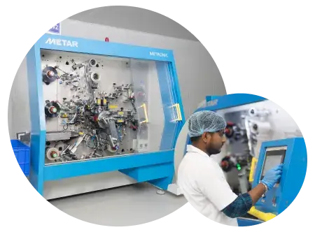
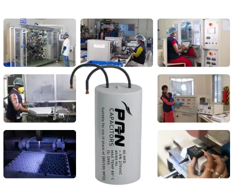
PAN Electronics has invested in state-of-the-art infrastructure for Metalized Capacitor Film production and Capacitor Manufacturing with advanced machinery and process discipline.
Sq.ft integrated facility at Peenya, Bengaluru.
World class metalization lines.
10,000 clean-room controlled slitting setup.
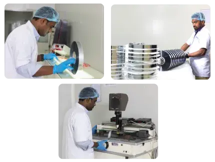
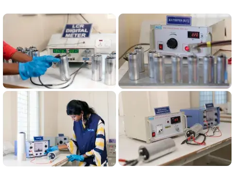
Dedicated inspection labs for process control.
PAN Electronics has invested in state-of-the-art infrastructure for their Metalized Capacitor Film Production line and Capacitor Manufacturing line. With cutting-edge technology and advanced equipment, we ensure that our products meet the highest standards of quality and performance.
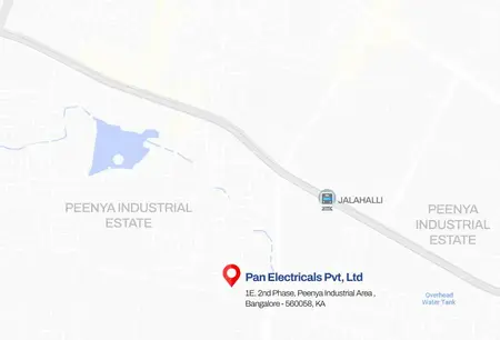
The PAN Electronics factory is spread over 100,000 Sq.ft and strategically located in Bengaluru; famous of its Information and Technology process. The factory site is situated in Peenya regarded as the biggest industrial areas in Asia. The plant lies close to the Bangalore-Tumkur Highway ensuring easy accessibility to transport via Road.
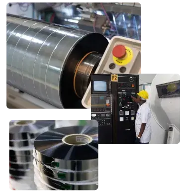
BOPP film which is imported from Toray and Honshu (Japan) and Hoechst (Germany) other than Korean & European Countries.
For standard products, custom builds and MPP film requirements.
Enquire NowApply for electronic capacitor product samples.
Request NowBrowse brochures, flyers and technical material from PAN.
Download NowPartner with PAN and explore distribution-led growth.
Contact UsPAN Electronics manufactures capacitor solutions and metallised polypropylene dielectric films for appliance, industrial and power-factor applications with a quality-led production approach.
©2025. All Rights Reserved. Designed and maintained by IRDM ![]()